Completed Projects
Projects completed before Fall 2013 (formation of EEMS Group)
![]()

HEVC/H.265 Video Coding Standard Development
with Madhukar Budagavi and Minhua Zhou @ Texas Instruments
September 2010 – January 2013
High Efficiency Video Coding (HEVC) was developed by the Joint Collaborative Team for Video Coding (JCT-VC). It delivers up to a 50% higher coding efficiency compared to its predecessor H.264/AVC. HEVC uses several new tools for improving coding efficiency, including larger block and transform sizes, additional loop filters, and highly adaptive entropy coding. While high coding efficiency is important for reducing the transmission and storage cost of video, processing speed, power consumption and area cost also need to be considered in the development of next-generation video coding to handle the demand for higher resolution and frame rates.
Related Publications: Standards Contributions, ICIP2011, PCS2012, SPIE2012, ICIP2012, ICIP2012, ICIP2012, TCSVT2012, SIPS2013, J-STSP2013, J-STSP2013, Springer Book on HEVC
Research below was done in the Energy-Efficient Integrated Circuits and Systems Group @ MIT under the guidance of Anantha P. Chandrakasan
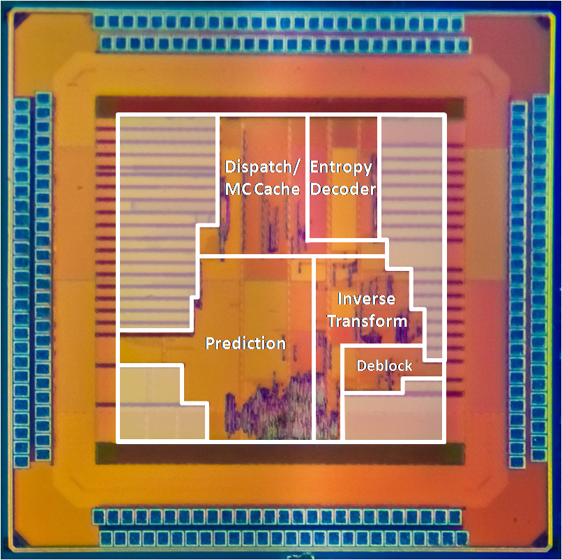
HEVC Video Decoder for 4K Ultra HD Applications
with Chao-Tsung Huang, Mehul Tikekar, and Chiraag Juvekar
March 2012
A video decoder chip supporting the High Efficiency Video Coding (HEVC) standard is designed in 40nm CMOS. The chip runs at 200 MHz at 0.9V with a throughput of 249 Mpixel/s to meet the requirements of 4K Ultra HD applications. Various architectural innovations are implemented in the chip to address large and variable pixel block sizes in HEVC and longer interpolation filters compared to the previous H.264/AVC standard. A motion compensation cache is designed to reduce the average bandwidth required from external memory by 67%. The chip consumes 78mW when decoding video at a resolution of 3840×2160 at 30 frame/s. The total system efficiency including simulated DRAM power is 1.19 nJ/pixel.
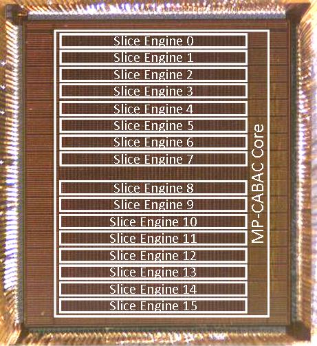
Low Power Algorithms and Architectures for Next Generation Video Coding Standard
Ph.D. Research
October 2009
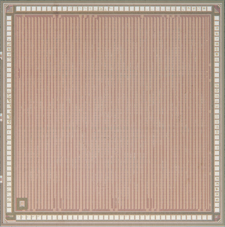
A prototype of a pre-standard algorithm developed for HEVC called Massively Parallel CABAC that addresses a key bottleneck in the video decoder is implemented in a 65-nm CMOS process. The scalable testchip achieves a throughput of 24.11bin/cycle, which enables it to decode the max H.264/AVC bitrate (300Mb/s) with a 18MHz clock at 0.7V, consuming 12.3pJ/bin. At 1.0V, it decodes a peak of 3026Mbin/s for a bit-rate of 2.3Gb/s, which is enough for over seven 300Mb/s sequences or a 4kx2k resolution video at 186 frame/s. Joint algorithm and architecture optimizations are used to reduce critical path delay and memory requirements with little or no cost in coding efficiency.
Related Publications: ICIP2008, TCSVT2009, ISSCC2011, ICASSP2011, JSSC2012, JSPS2012
Low Power Real-time H.264/AVC HD Video Decoding System
Ph.D. Research
with Daniel Finchelstein and Mahmut Sinangil
April 2008
The H.264/AVC Baseline Level 3.2 decoder was designed in 65-nm CMOS. It can operate at 0.7 V for high definition (1280×720 at 30 frame/s) video decoding and with a measured power of 1.8 mW, which is over an order of magnitude lower than previously published results. Power reduction is achieved through architectural optimizations such as increased parallelism, multiple voltage / frequency domains and custom voltage-scalable SRAMs.
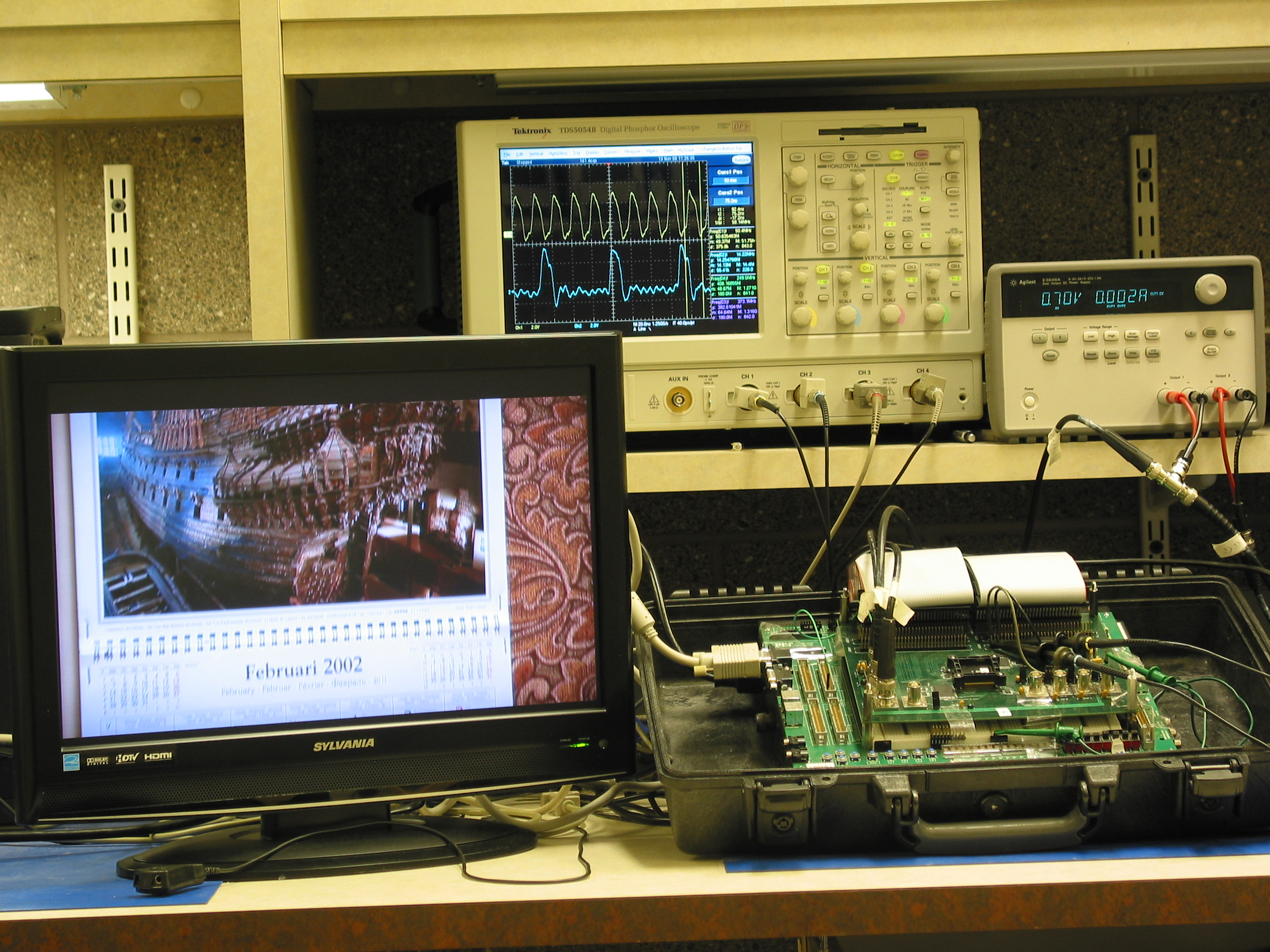
Description of video (above)
- High definition 720p mobcal sequence playback at 30 frames per second.
- PCB with H.264/AVC decoder test chip (black square socket in center).
Decoded video goes through ribbon cables to VGA socket to LCD display. - Clock signals on scope: Top (yellow) is the core 14 MHz clock.
Bottom (blue) is the memory controller 50 MHz clock. - Core domain consumes <1mW from a 0.73 V power supply.
- Real-time 720p 30fps, H.264/AVC video playback system.
Outstanding Design Award, 2008 Asian Solid-State Circuits Conference Student Design Contest
Please visit the Portable Multimedia Group website for more info.
Related Publications: A-SSCC2008, JSSC2009, ProcIEEE2010
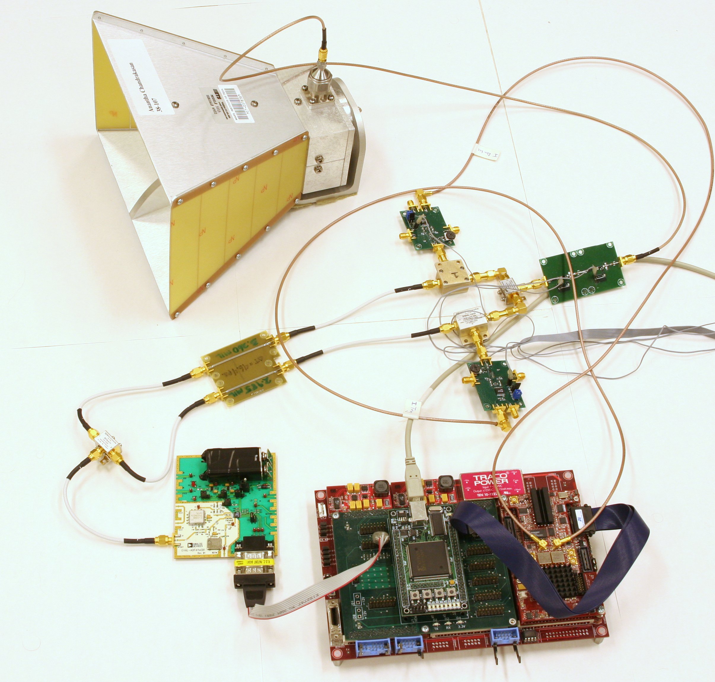
Ultra-Low Voltage UWB Baseband Processor
S.M. Research
September 2006
The baseband processor performs acquisition and demodulation of an UWB packet with a throughput of 500-MS/s for a data-rate of 100-Mb/s. It operates at an ultra-low supply voltage of 400-mV to achieve 20 pJ/bit, and utilizes a highly parallelized architecture (with 620 complex correlators) to meet throughput constraints. It was fabricated in a standard-VT 90-nm CMOS process.
Winner, 2007 Design Automation Conference (DAC)/ International Solid-State Circuits Conference (ISSCC) Student Design Contest
Please visit the Sub-Threshold Circuits Group website for more info.
Related Publications: ICASSP2006, ISLPED2007, ProcIEEE2009
A 50Mb/s UWB Prototype Transceiver
S.M. Research
with Nathan Ackerman, Raul Blazquez, Kyle Gilpin, Brian Ginsburg, Fred Lee, and David Wentzloff
August 2005
This prototype transceiver is built using discrete components. It communicates in a 500MHz band centered at 5.355GHz using BPSK pulses with a pulse repetition frequency of 50MHz. The received signal is down-converted to I/Q baseband signals using off-the-shelf discrete components. The baseband signals are digitized by dual 8-bit Atmel ADCs. Synchronization and demodulation are implemented in a Xilinx Virtex II FPGA enabling real-time communication at 50Mb/s. The transceiver communicates with a PC over USB2.0. Real-time one-way transmission of a video stream over the air has been demonstrated at a 50Mb/s raw data rate using this transceiver.
Please visit the Ultra-Wideband Project website for more info.
Related Publications: IEEEComMag2005