Events
Non-contact Nondestructive Probing of Charge Carrier Conductivity in Organic Materials and their Interfaces
January 15, 2015 at 3:30pm/ 4-270
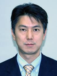
Shu Seki
Osaka University

Abstract:
Understanding charge carrier transport processes at interfaces is one of the most important subjects in organic electronics. Charge carriers are injected or extracted through metal/semiconductor interfaces in most electronic devices, while carrier transport occurs at insulator/semiconductor interfaces rather than in the bulk in the major organic electronic devices.1,2 However, analytical techniques for evaluating such interfacial carrier transport phenomena are still limited, and this remains a challenging issue. We have recently reported a technique, referred to as time-resolved microwave conductivity (TRMC)3, and the system has been extended into field-induced TRMC that combines charge carrier injection via gate bias applied into working devices and microwave-based non-contact probing of intrinsic and local charge carrier motion. The schematic diagram of the set of apparatus is given in figure 1. Using this technique, it was determined that a Au/pentacene/PMMA/SiO2/Au MIS device had hole and electron mobilities of 6.3 and 0.3 cm2V–1s–1, respectively.4,5 Non-contact, fully experimental evaluation of intra-domain carrier mobility at interfaces is quite unprecedented and is a characteristic feature of this system. In this paper, we further report that the FI-TRMC technique can distinguish between mobile charge carriers at the interface and immobile charges trapped at defects, thus enabling quantification of both the charge carrier mobility and the density of trap sites at insulator-semiconductor interfaces, and discuss also on the extraordinary mobile charge carriers at the interfaces on highly developed planner -conjugated systems such as graphene and its derivatives.
References: 1) G. Horowitz and P. Delannoy, J. Appl. Phys. 70, 469 (1991). 2) H. Klauk, Chem. Soc. Rev. 39, 2643 (2010). 3) S. Seki, et al., Phys. Chem. Chem. Phys. 16, 11093 (2014); Acc. Chem. Res. 45, 1193 (2012); Nature Commun. 5, 3718 (2014); Nature Commun. 4, 2694 (2013); Nature Commun. 4, 1691 (2013); 4) S. Seki, et al., Sci. Rep. 3, 3182 (2013). 5) W. Choi, T. Miyakai, T. Sakurai, A. Saeki, M. Yokoyama, S. Seki, Appl. Phys. Lett. 105, 019430 (2014)
Bio:
Shushi Seki received his BS (1991) and MS (1993) in Engineering at the University of Tokyo. In 1995, he worked in the Chemistry Division at the Argonne National Laboratory . He was Assistant Professor at Osaka University, Japan, from 1995 – 2001 while earning his PhD in 2001. From 2001 – 2007, he was an Associate Professor at the Institute of Scientific and Industrial Research and from 2007-2009, at the Department of Applied Chemistry, both at Osaka University. Currently, he is Professor in the Department of Applied Chemistry Graduate School of Engineering at Osaka and his area of research is in condensed matter physical chemistry.


