
Yunjo Kim1, Samuel S. Cruz, Kyusang Lee, Babatunde O. Alawode, Chanyeol Choi, Yi Song, Jared M. Johnson, Christopher Heidelberger, Wei Kong, Shinhyun Choi, Kuan Qiao, Ibraheem Almansouri1, Eugene A. Fitzgerald, Jing Kong, Alexie M. Kolpak, Jinwoo Hwang, & Jeehwan Kim
doi:10.1038/nature22053
Abstract:
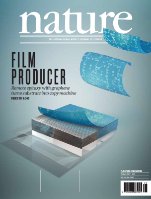
Epitaxy—the growth of a crystalline material on a substrate—is crucial for the semiconductor industry, but is often limited by the need for lattice matching between the two material systems. This strict requirement is relaxed for van der Waals epitaxy1, 2, 3, 4, 5,6, 7, 8, 9, 10, in which epitaxy on layered or two-dimensional (2D) materials is mediated by weak van der Waals interactions, and which also allows facile layer release from 2D surfaces3, 8. It has been thought that 2D materials are the only seed layers for van der Waals epitaxy3, 4, 5, 6, 7, 8, 9, 10. However, the substrates below 2D materials may still interact with the layers grown during epitaxy (epilayers), as in the case of the so-called wetting transparency documented for graphene11, 12, 13. Here we show that the weak van der Waals potential of graphene cannot completely screen the stronger potential field of many substrates, which enables epitaxial growth to occur despite its presence. We use density functional theory calculations to establish that adatoms will experience remote epitaxial registry with a substrate through a substrate–epilayer gap of up to nine ångströms; this gap can accommodate a monolayer of graphene. We confirm the predictions with homoepitaxial growth of GaAs(001) on GaAs(001) substrates through monolayer graphene, and show that the approach is also applicable to InP and GaP. The grown single-crystalline films are rapidly released from the graphene-coated substrate and perform as well as conventionally prepared films when incorporated in light-emitting devices. This technique enables any type of semiconductor film to be copied from underlying substrates through 2D materials, and then the resultant epilayer to be rapidly released and transferred to a substrate of interest. This process is particularly attractive in the context of non-silicon electronics and photonics, where the ability to re-use the graphene-coated substrates8 allows savings on the high cost of non-silicon substrates.