Research
A Novel Sublimable Mask Lift-off Method for Patterning Thin Films of Organic Semiconductors
M. E. Bahlke, H. A. Mendoza, M. A. Baldo
Sponsorship: MITEI Graduate Fellowship in Energy, MIT Center for Excitonics DOE Office of Basic Energy Sciences EFRC
Photolithography’s accuracy and scalability have made it the method for sub-micron-scale definition of single-crystal semiconductor devices for over half a century. Unfortunately, organic semiconductor devices are chemically incompatible with the types of resists, solvents, and etchants traditionally used. This work investigates the use of an uncommonly used chemically inert resist method [1]-[5] that relies on physical phase changes for lift-off patterning of thin films of organic semiconductors and metals.
The resist gas is flowed over a cryogenically cooled substrate, where it freezes solid. This layer can be patterned by thermal excitation in a number of ways to define the areas where the desired thin film is to remain. After the desired thin film or films are deposited, the substrate is brought up above the resist material’s sublimation point, leaving behind only the intended pattern. All the unwanted regions are lifted-off by the subliming resist.
Creating and defining the shadow mask on the surface of the substrate in this manner allow for patterning it with a stamp or roller with micron-scale features without changing the process conditions. In this work, carbon dioxide is used as the sublimable mask material, and prototype stamps have been fabricated using SU-8 photoresist. A mask and the subsequent organic thin film are shown in Figure 2. This process may provide an alternative to shadow masks and provide a manufacturing solution for large area organic electronics.
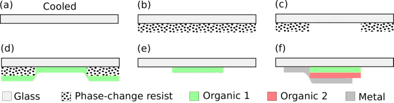
Fig. 1 Simplified process flow for sublimation lithography (not to scale). (a) Begin with a cooled substrate to facilitate resist deposition. (b) Deposit resist. (c) Selectively pattern resist. (d) Deposit desired thin film. (e) Lift-off resist leaving patterned thin film. (f) Repeat as necessary to complete device.
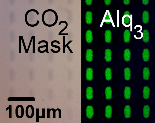
Fig. 2 Optical micrograph of a patterned sublimable mask of carbon dioxide(left). Photoluminescence of the resulting organic thin film after deposition and lift-off(right).
Relevant Publications
- W. Johnson, R. Laibowitz, and C. Tsuei, “Condensed gas, in situ lithography,” IBM Technical Disclosure Bulletin, vol. 20, no. 9, Feb. 1978.
- A. Han, D. Vlassarev, J. Wang, J. A. Golovchenko, and D. Branton, “Ice lithography for nanodevices,” Nano Letters, vol. 10, no. 12, pp. 5056-5059, Dec. 2010.
- D. Branton, J. A. Golovchenko, G. M. King, W. J. MoberlyChan, and G. M. Schürmann, “Lift-off patterning processing employing energetically-stimulated local removal of solid-condensed-gas layers” U.S. Patent 752443 B1, April 28, 2009.
- G. M. King, G. Schürmann, D. Branton, and J. A. Golovchenko, “Nanometer patterning with ice,” Nano Letters, vol. 5, no. 6, pp. 1157-1160, June 2005.
- J. Cuomo, C. Guarnieri, K. Saenger, and D. Yee, “Selective deposition with ‘dry’ vaporizable lift-off mask,” IBM Technical Disclosure Bulletin, vol. 35, no. 1, June 1992.
- Matthias E. Bahlke, Hiroshi A. Mendoza1, Daniel T. Ashall, Allen S. Yin, Marc A. Baldo, “Dry Lithography of Large-Area, Thin-Film Organic Semiconductors Using Frozen CO2 Resists,” Advanced Materials, Sept. 2012.