Research
Nanoelectromechanical Memories and Switches
All Graphene Electromechanical Switch Fabricated by Chemical Vapor Deposition
K.M. Milaninia, A. Reina, J. Kong, and M.A. Baldo
Sponsorship: FCRP IFC, DARPA
Nanoelectromechanical switches (NEMS) exhibit minimal leakage current in the off state because of both low subthreshold leakage current and gate leakage current. Consequently, they may find application in low power electronics. This work focuses on the fabrication of a double layer graphene switch. We demonstrate an electromechanical switch comprising two polycrystalline graphene films, each deposited using ambient pressure chemical vapor deposition (CVD). Large area graphene sheets facilitate the use of straight forward “top-down” fabrication of electromechanical switches. The top film is pulled into electrical contact with the bottom film by application of approximately 5V between the layers. Contact is broken by mechanical restoring forces after bias is removed. The device switches several times before tearing. Demonstration of multiple switching at low voltage and large on currents confirms that graphene is an attractive material for electromechanical switches. Reliability may be improved by scaling the device area to within one crystalline domain of the graphene films.
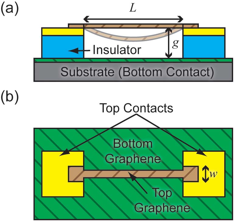
Figure 1: Schematic diagram of an all CVD graphene switch from (a) a cross sectional view and (b) a top view. The device consists of two layers of CVD-grown graphene. The bottom graphene is placed on a conductive substrate which functions as a bottom contact. The top graphene film is patterned into a beam with a length and width of L = 20 μm and w = 3 μm, respectively, and suspended above the bottom contact by a gap, g = 500 nm. The top graphene beam is held in place via two top metal contact electrodes. The switch is activated through the application of a bias between top and bottom contacts.
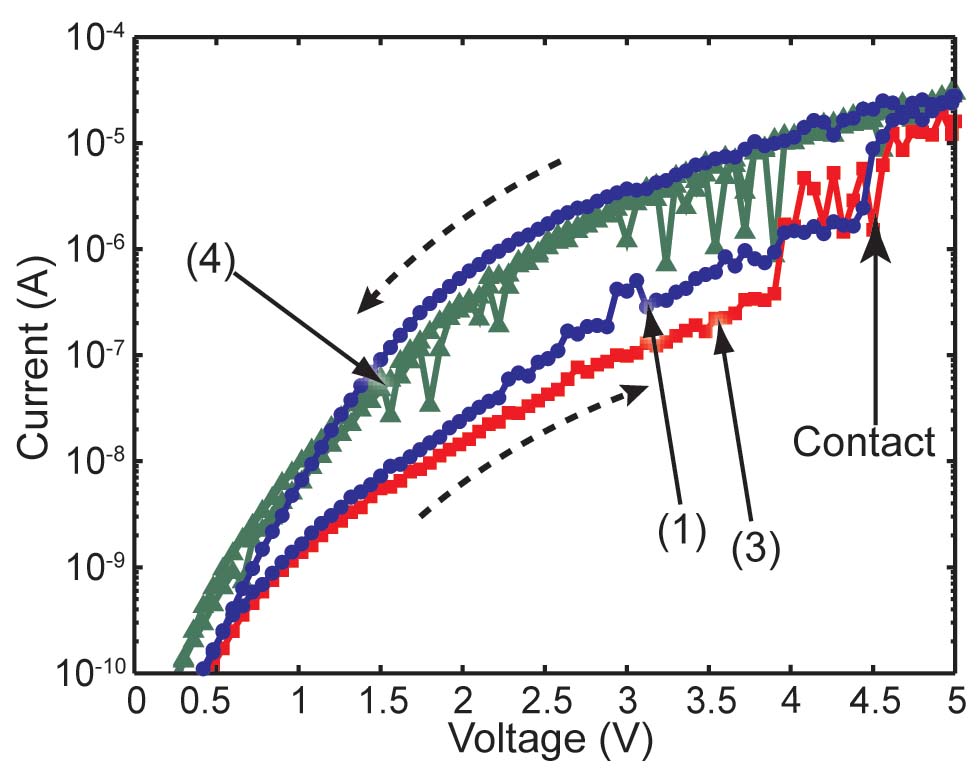
Figure 2: Current-Voltage characteristics between the top and bottom contacts for a w = 3 μm, L = 60 μm device showing multiple switching transitions: (1) first scan, (3) third scan (plotted only from 0 V to 5 V), and (4), the fourth and final scan.