Max M. Shulaker, Gage Hills , Rebecca S. Park , Roger T. Howe , Krishna Saraswat , H.-S. Philip Wong & Subhasish Mitra
doi:10.1038/nature22994
Abstract:
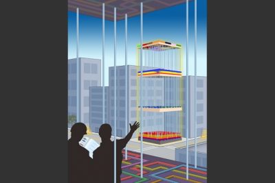
The computing demands of future data-intensive applications will greatly exceed the capabilities of current electronics, and are unlikely to be met by isolated improvements in transistors, data storage technologies or integrated circuit architectures alone. Instead, transformative nanosystems, which use new nanotechnologies to simultaneously realize improved devices and new integrated circuit architectures, are required. Here we present a prototype of such a transformative nanosystem. It consists of more than one million resistive random-access memory cells and more than two million carbon-nanotube field-effect transistors—promising new nanotechnologies for use in energy-efficient digital logic circuits1, 2, 3 and for dense data storage4—fabricated on vertically stacked layers in a single chip. Unlike conventional integrated circuit architectures, the layered fabrication realizes a three-dimensional integrated circuit architecture with fine-grained and dense vertical connectivity between layers of computing, data storage, and input and output (in this instance, sensing). As a result, our nanosystem can capture massive amounts of data every second, store it directly on-chip, perform in situ processing of the captured data, and produce ‘highly processed’ information. As a working prototype, our nanosystem senses and classifies ambient gases. Furthermore, because the layers are fabricated on top of silicon logic circuitry, our nanosystem is compatible with existing infrastructure for silicon-based technologies. Such complex nano-electronic systems will be essential for future high-performance and highly energy-efficient electronic systems5.
