Research
Research Area III: Active Devices - Photonic Microsystems Group
1.8.2015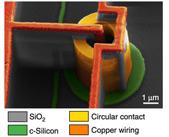
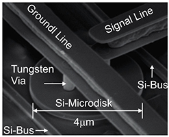
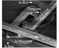
The continued Moore’s Law scaling of transistor density is outstripping the capacity of electrical communication lines both on and off high-performance CMOS chips. Off-chip communications, limited by pin-density, serialization speeds, the numer of board layers, and ultimately the communications efficiency (energy/bit), present the most pressing concerns. Without increased inter-chip communications bandwidth at reduced power consumption, high-performance computers will become increasingly imbalanced (bytes/FLOPs<<1) resulting in substantially degraded real-world application performance. Silicon microphotonics offers a solution to the communications bottlenecks in high-performance CMOS circuits enabling ultralow power terabit-per-second communication lines on-chip using wavelength-division-multiplexing (WDM). Here in our group, we utilize depletion-based resonant modulators, which use vertical p-n junctions, interior electrical contacts, and a hard outer resonator wall. The hard outer wall and interior electrical contacts enabled small footprint (<3.5um) and low energy consumption of the modulators (left and middle figures). Moreover, within the same process, high-speed silicon bandpass switches (right figure) were also demonstrated, which offer potential for low-power high-speed optical domain routing of WDM signals as well as thermal tuners to heat the silicon directly for fast and efficient thermal tuning. While 1fJ/bit modulators and optical switches are not needed today, with the exponential scaling presented by Moore’s Law, these results represent an important path towards ultra-efficient inter- and intra-chip communications that will be available to system and chip designers of the future.