Research - Photonic Microsystems Group
Research Topic Areas
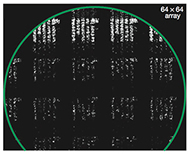
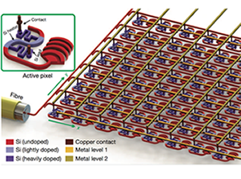
Research Area I: Phased Arrays
Videos:
Research Area II: On-Chip Lasers & Integration
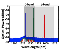
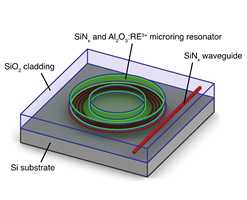
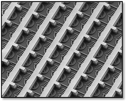
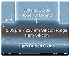
The ability to reliably fabricate silicon microphotonic devices and systems in a CMOS-compatible process is the key to the success of silicon photonics. Our group established a collaboration with the College of Nanoscale Science and Engineering (CNSE) at the University of Albany. Together we developed the first 300mm silicon photonics process ever demonstrated. The process flow itself consists of two etch steps in the silicon layer, four implants, two dual damascene copper interconnect and via layers, three layers of silicon nitride, germanium, etched facets for low-loss coupling, and a trench etch for the incorporation of an active erbium doped layer for on-chip lasers and optical amplifiers. Using this recently developed process flow, our group has demonstrated erbium-doped lasers in a manner that allows for direct integration of lasers on-chip (left figure). Already, distributed feedback (DFB) and distributed Bragg reflector (DBR) lasers have been demonstrated on-chip across a broad range of wavelengths and with output powers as high as 75mW and in passive demonstrations, channel alignment to within 10-picometers has been achieved (middle figure). Besides, microdisk cavity laser (right figure) has also been demonstrated as a compact (~80um radius) on-chip laser source. To achieve future advances, rigorous electromagnetic design must be coupled to CMOS circuitry to drive, minitor, and control the performance of the microphotonic circuits and networks. The approach used in our group utilize wafer-sacle 3D integration with through oxide vias that enable the high-densities and low parasitics offered by direct integration while maintaining the flexibility to separately optimize the photonics and CMOS processes common to hybrid integration techniques.
Research Area III: Active Devices
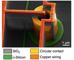
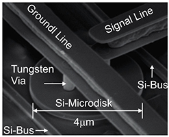
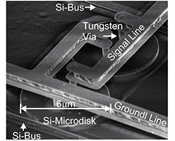
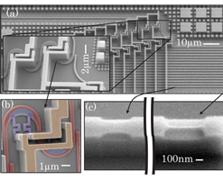
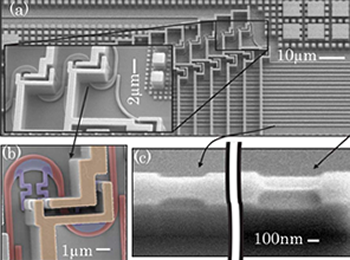
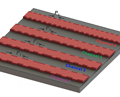
The continued Moore’s Law scaling of transistor density is outstripping the capacity of electrical communication lines both on and off high-performance CMOS chips. Off-chip communications, limited by pin-density, serialization speeds, the numer of board layers, and ultimately the communications efficiency (energy/bit), present the most pressing concerns. Without increased inter-chip communications bandwidth at reduced power consumption, high-performance computers will become increasingly imbalanced (bytes/FLOPs<<1) resulting in substantially degraded real-world application performance. Silicon microphotonics offers a solution to the communications bottlenecks in high-performance CMOS circuits enabling ultralow power terabit-per-second communication lines on-chip using wavelength-division-multiplexing (WDM). Here in our group, we utilize depletion-based resonant modulators, which use vertical p-n junctions, interior electrical contacts, and a hard outer resonator wall. The hard outer wall and interior electrical contacts enabled small footprint (<3.5um) and low energy consumption of the modulators (left and middle figures). Moreover, within the same process, high-speed silicon bandpass switches (right figure) were also demonstrated, which offer potential for low-power high-speed optical domain routing of WDM signals as well as thermal tuners to heat the silicon directly for fast and efficient thermal tuning. While 1fJ/bit modulators and optical switches are not needed today, with the exponential scaling presented by Moore’s Law, these results represent an important path towards ultra-efficient inter- and intra-chip communications that will be available to system and chip designers of the future.
Research Area IV: Passive Devices
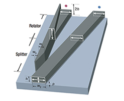
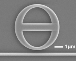
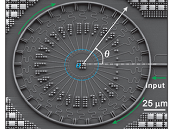
Research in the electromagnetic design of microphotonic elements offers potential for new nanoscale electromagnetic field manipulations, light-matter interactions, plasmonic and metamaterial effects, and sensing modalities. As a result, some of the most interesting physics extends from single devices. Example structures being developed in our group include the polarizition rotator and splitter (left figure) with the ability to rotate polarization states through structural chirality and split polarization states through mode evolution. Moreover, rigorous electromagnetic design led to tolerant structures, along with the ability to filter optical signals with high-fidelity through coupled microring-resonator filters, enabling the first demonstration of a polarization independent microphotonic circuit, a key result proving the potential of microphotonics for optical communications. Finally, through a careful manipulation of Maxwell’s equations, we discovered the only radiation-free nanophotonic cavities without a complete photonic bandgap. In addition, the group developed some first-of-its-kind microphotonic elements, including adiabatic microring resonators (middle figure) which provide electrical or mechanical contacts with little harm on the quality factors. Besides, the wafer-scale resonance variations of this type of filter are reduced by 2 times compared to conventional ring resonators. More recently, we continued to extend the performance of passive components. Through a careful design approach and fabrication strategy, our group has achieved ring-resonators with high Q (2.2e7) (right figure), which representing a new record low loss silicon (0.027dB/cm). In all of the cases, rigorous electromagnetic design, has, and will continue to play a pivotal role in the research of my group. Much as the transistor drove microelectronics, microphotonic elements will drive new circuits, systems, and networks.