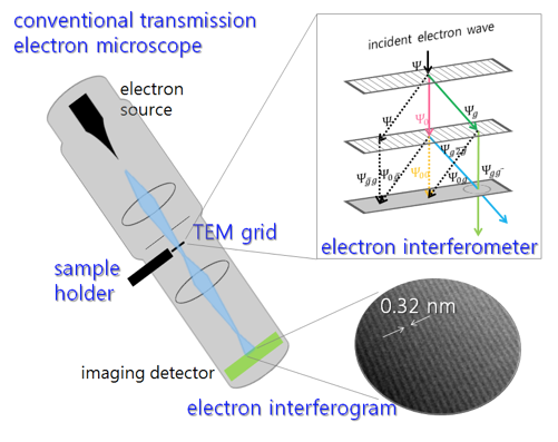
We describe a modular, self-aligned, amplitude-division electron interferometer in a conventional transmission electron microscope. The interferometer consists of two 45-nm-thick silicon layers separated by 20 μm. This interferometer is fabricated from a single-crystal silicon cantilever on a transmission electron microscope grid by gallium focused-ion-beam milling. Using this interferometer, we obtain interference fringes in a Mach-Zehnder geometry in an unmodified 200 kV transmission electron microscope. The fringes have a period of 0.32 nm, which corresponds to the [1̄1̄1] lattice planes of silicon, and a maximum contrast of 15%. We use convergent-beam electron diffraction to quantify grating alignment and coherence. This design can potentially be scaled to millimeter-scale, and used in electron holography. It could also be applied to perform fundamental physics experiments, such as interaction-free measurement with electrons. A complete description of the work may be found here.

Citation:
Akshay Agarwal, Chung-Soo Kim, Richard Hobbs, Dirk van Dyck and Karl K. Berggren. “A nanofabricated, monolithic, path-separated electron interferometer,” Scientific Reports, 7, 1677 (2017) . DOI: 10.1038/s41598-017-01466-0