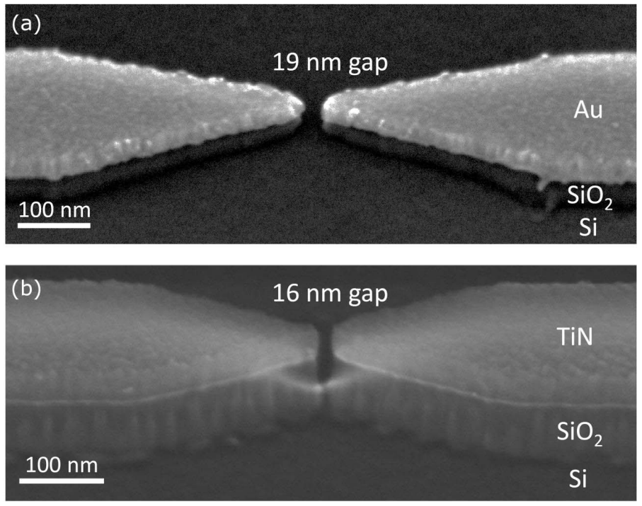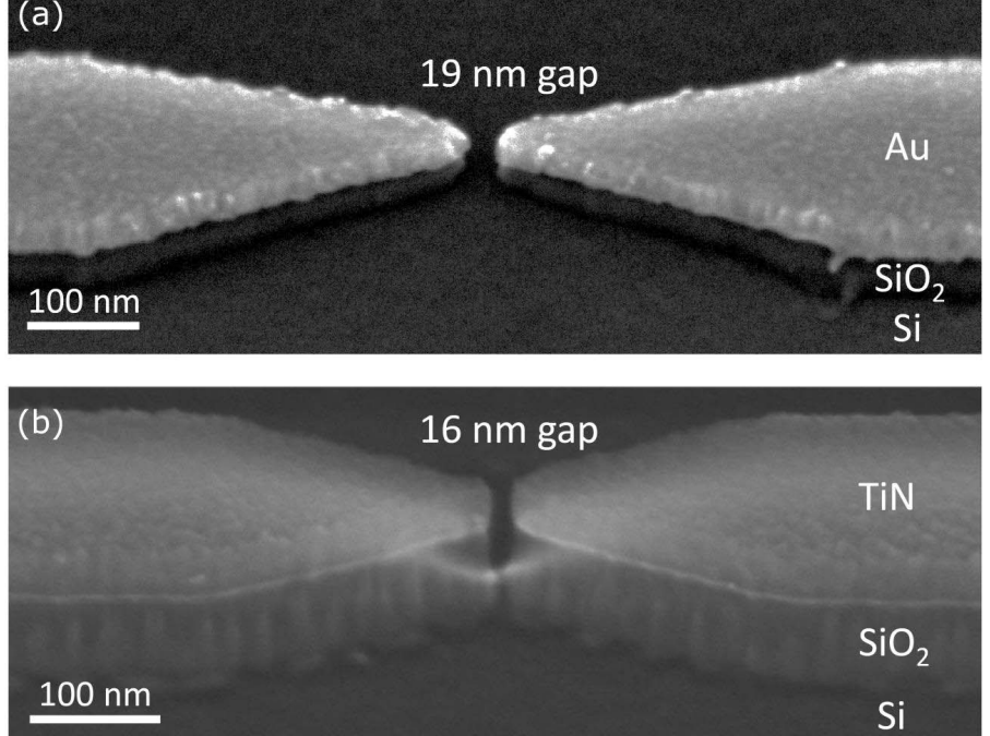
Recent advancements in nanofabrication have enabled the creation of vacuum electronic devices with nanoscale free-space gaps. These nanoelectronic devices promise the benefits of cold-field emission and transport through free space, such as high nonlinearity and relative insensitivity to temperature and ionizing radiation, all while drastically reducing the footprint, increasing the operating bandwidth, and reducing the power consumption of each device. Furthermore, planarized vacuum nanoelectronics could easily be integrated at scale similar to typical microscale and nanoscale semiconductor electronics. However, the interplay between different electron emission mechanisms from these devices is not well understood, and inconsistencies with pure Fowler-Nordheim (FN) emission have been noted by others. In this work, we systematically study the current-voltage characteristics of planar vacuum nanodevices having few-nanometer radii of curvature and free-space gaps between the emitter and the collector. By investigating the current-voltage characteristics of nearly identical devices fabricated from two different materials and under various environmental conditions, such as temperature and atmospheric pressure, we are able to clearly isolate three distinct emission regimes within a single device: Schottky, FN, and saturation. Our work will enable robust and accurate modeling of vacuum nanoelectronics, which will be critical for future applications requiring high-speed and low-power electronics capable of operation in extreme conditions.
A complete description of the work may be found here.