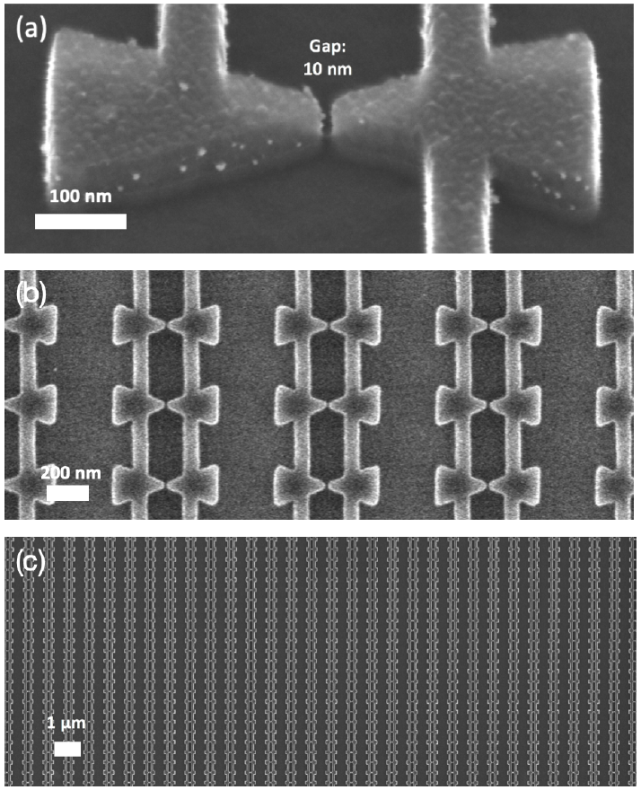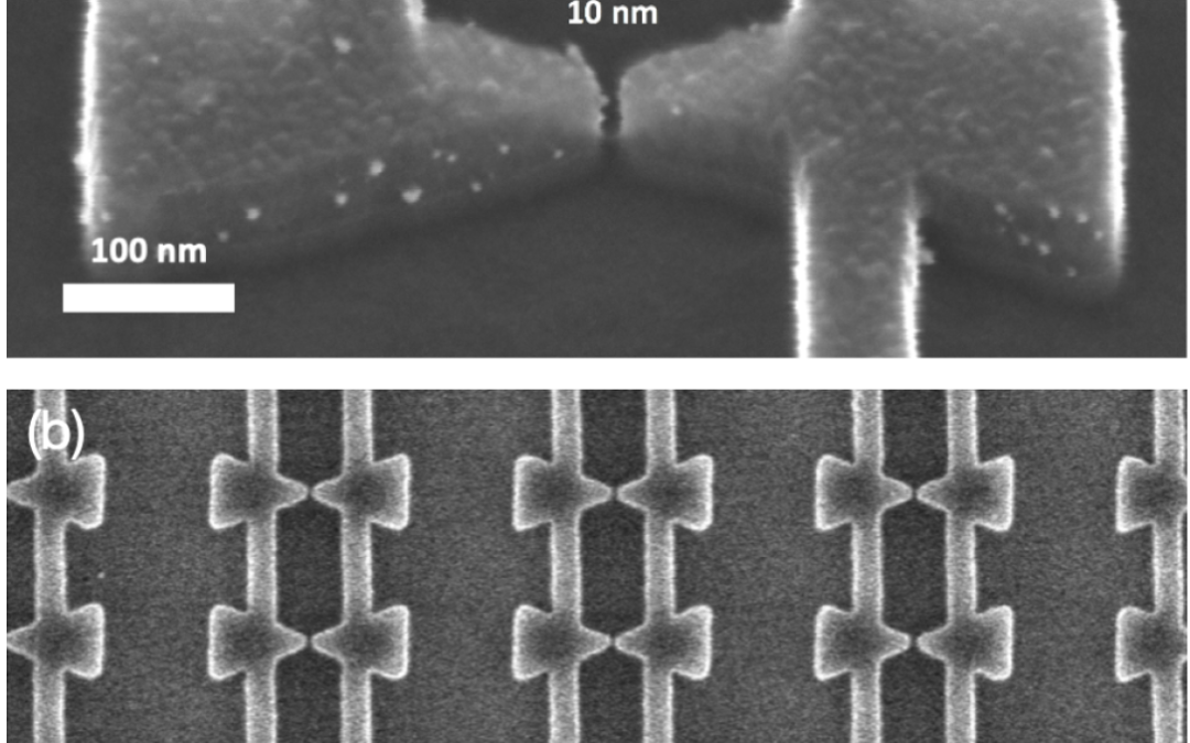
Refractory materials exhibit high damage tolerance, which is attractive for the creation of nanoscale field-emission electronics and optoelectronics applications that require operation at high peak current densities and optical intensities. Recent results have demonstrated that the optical properties of titanium nitride, a refractory and CMOS-compatible plasmonic material, can be tuned by adding silicon and oxygen dopants. However, to fully leverage the potential of titanium (silicon oxy)nitride, a reliable and scalable fabrication process with few-nm precision is needed. In this work, we developed a fabrication process for producing engineered nanostructures with gaps between 10 and 15 nm, aspect ratios larger than 5 with almost 90° steep sidewalls. Using this process, we fabricated large-scale arrays of electrically-connected bow-tie nanoantennas with few-nm free-space gaps. We measured a typical variation of 4 nm in the average gap size. Using applied DC voltages and optical illumination, we tested the electronic and optoelectronic response of the devices, demonstrating sub-10-V tunneling operation across the free-space gaps, and quantum efficiency of up to 1centerdot10-3 at 1.2 μm, which is comparable to a bulk silicon photodiode at the same wavelength and three orders of magnitude higher than with nearly identical gold devices. Tests demonstrated that the titanium silicon oxynitride nanostructures did not significantly degrade, exhibiting less than 5 nm of shrinking of the average gap dimensions over few-μm2 areas after 10 hours of operation. Our results will be useful for developing the next generation of robust and CMOS-compatible nanoscale devices for high-speed and low-power field-emission electronics and optoelectronics applications.
A complete description of the work may be found here.