Facilities
We are members of the Center for Excitonics, Microsystems Technology Laboratories (MTL), and Research Laboratory of Electronics (RLE). In addition to those shared resources, we maintain some additional facilities within our group.
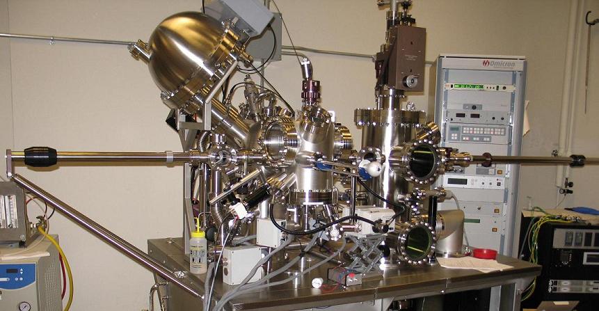
Ultra high vacuum (UHV) System
The UHV system is used to grow devices with stringent purity requirements. In situ growth and characterization of devices is done at pressures down to 10-11 Torr. The system is used for scanning probe microscopy (SPM), molecular beam epitaxy (MBE), ultraviolet photoelectron spectroscopy (UPS), and current-voltage characterization. SPM techniques possible in the system are: scanning tunneling microscopy (STM), atomic force microscopy (AFM), Kelvin probe force microscopy (KPFM). Measurements can be done over a temperature range of 25K to 1500K. The MBE system was designed and built by in-house. The surface analysis components were purchased from Omicron.
Fig. 1 UHV system
Fabrication Laboratory
The fabrication laboratory contained in 13-3135, a class 1000 cleanroom, includes a computer controlled vacuum thermal evaporator with a base pressure of 10-8 Torr and 6 sources (in three independent pairs). The chamber is built into a moisture and oxygen free dry box to prevent atmospheric contamination. This glove box is attached to a second dedicated glove box with spinner and vacuum oven is available for solution processing of polymeric materials.
Fig. 2 Glove box – the thermal evaporator is behind the left window
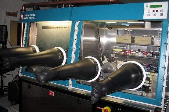
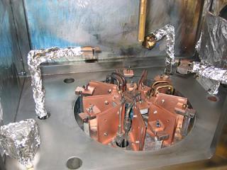
Fig. 3 Close up of thermal evaporator
The evaporator is capable of depositing gold, chromium, aluminum and a variety of other metals, as well as evaporable soft semiconductors. The system was built by Angstrom Engineering. Additional equipment includes a chromatography refrigerator, two -80º freezers, and an ultracentrifuge.
Optical Characterization Laboratory
The characterization laboratory contained in 26-440 contains a variety of optical and electrical test and measurement facilities including a solar simulator, automated wavelength-resolved or angle-resolved photocurrent detection, dye and solid state lasers, and two He cryostats: one for optical measurements, and a second with four micro-positioned electrical probes.