Timothy William Jones, Anna Osherov, Mejd Alsari, Melany Sponseller, Ben C Duck, Young-Kwang Jung, Charles Settens, Farnaz Niroui, Roberto Brenes, Camelia Stan, Yao Li, Mojtaba Abdi-Jalebi, Nobumichi Tamura, J. Emyr Macdonald, Manfred Burghammer, Richard Friend, Vladimir Bulovic, Aron Walsh, Gregory Joseph Wilson, Samuele Lilliu and Samuel D Stranks
DOI: 10.1039/C8EE02751J
Abstract:
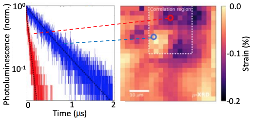
Halide perovskites are promising semiconductors for inexpensive, high-performance optoelectronics. Despite a remarkable defect tolerance compared to conventional semiconductors, perovskite thin films still show substantial microscale heterogeneity in key properties such as luminescence efficiency and device performance. However, the origin of the variations remains a topic of debate, and a precise understanding is critical to the rational design of defect management strategies. Through a multi-scale investigation – combining correlative synchrotron scanning X‑ray diffraction and time-resolved photoluminescence measurements on the same scan area – we reveal that lattice strain is directly associated with enhanced defect concentrations and non-radiative recombination. The strain patterns have a complex heterogeneity across multiple length scales. We propose that strain arises during the film growth and crystallization and provides a driving force for defect formation. Our work sheds new light on the presence and influence of structural defects in halide perovskites, revealing new pathways to manage defects and eliminate losses.
