Abstract:
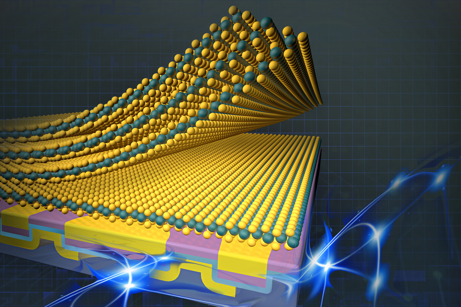
Pristine van der Waals (vdW) heterostructures formed between two-dimensional (2D) and other materials can be used to create optical and electronic devices. However, the weak vdW forces alone do not allow direct physical stacking of arbitrary layers. As a result, vdW heterostructure fabrication typically requires solvents, sacrificial layers or high temperatures, which can introduce damage and contaminants. Here, we show that adhesive matrix transfer can eliminate these limitations and can provide vdW integration beyond the limits of vdW forces. In the approach, a hybrid high- and low-adhesion surface is used to decouple the forces driving the transfer from the vdW forces defining the heterostructure of interest. We show that the technique can be used to achieve direct vdW integration of diverse 2D materials (MoS2, WSe2, PtS2 and GaS) with dielectrics (SiO2 and Al2O3), which is conventionally forbidden but critical for active devices and scalable, aligned heterostructure formation. The approach also allows single-step 2D material-to-device integration, which we illustrate by fabricating arrays of monolayer MoS2 transistors. As any exposure to solvents or polymers is avoided, the interfaces and surfaces remain pristine. Thus, intrinsic 2D material properties can be probed without the influence of processing steps. The materials can be further engineered through surface treatments and used to fabricate unconventional device form factors.
