
 It has been more than a century since the radio-frequency (RF) phased array radar was invented. Initially, the technology was adopted in military radar systems, and over time was also extended to many areas of application ranging from communication to astronomy. MIT’s Radiation Laboratory, the predecessor of the Research Laboratory of Electronics (RLE), was most famous for its radar research in World War II that played an important role in the Allied victory. Now RLE researchers demonstrate a phased array radar in optical frequency composed of 4,096 nanoantennas integrated on a small silicon chip. Notably, the chip is capable of generating arbitrary radiation patterns, and represents the largest optical phased array that has ever been demonstrated.
A phased array consists of several typically identical antennas, with each antenna emitting signals characterized by a specific amplitude and phase that interfere to form a certain radiation pattern in the far field. The ability to generate high-resolution and arbitrary radiation patterns with phased arrays has long been dreamt of and pursued by researchers. The capability will enable a broader range of applications from 3‑D holography to biomedical sensing, but requires a large-scale phased array with a considerable number of antennas. While the deployment of large-scale RF phased arrays is extremely cumbersome and expensive, its optical counterpart, the optical phased array, holds promise for large-scale integration attributed to the use of much shorter optical wavelength. The short optical wavelength nevertheless imposes stringent requirements on chip fabrication, as even nano-scale fluctuations in device dimensions significantly affect the optical emission from the nanoantennas. Consequently, all demonstrations of optical phased arrays so far have been restricted to 1‑D, or small-scale (16 antenna) 2‑D arrays.
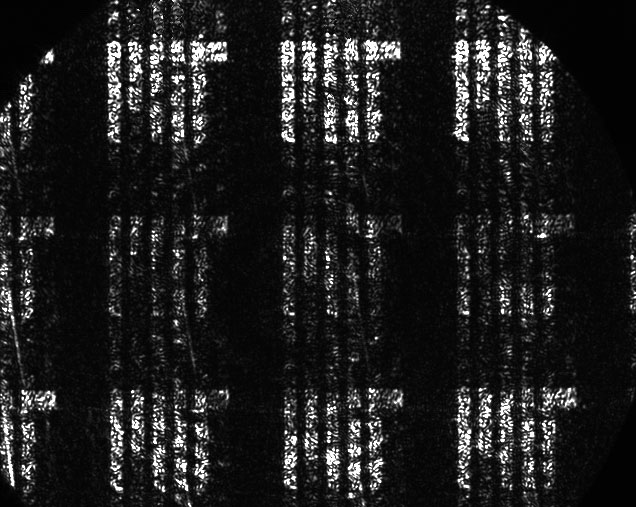
In the current issue of Nature (Vol. 493, No. 7431, pp. 195–199), RLE Prof. Michael R. Watts and graduate students Jie Sun, Erman Timurdogan, Ami Yaacobi, and postdoctoral associate Ehsan Shah Hosseini,report the demonstration of a large-scale, 2‑D nanophotonic phased array, in which 64 x 64 optical nanoantennas are integrated on a silicon chip. With a dense footprint of 576μmx576μm, the 4,096 nanoantennas are precisely balanced in power and aligned in phase to generate a designed and sophisticated radiation pattern. Furthermore, active phased arrays with the ability to generate dynamic radiation patterns in the far field have been experimentally demonstrated. The robust design of the array, coupled with state-of-the-art complementary metal-oxide-semiconductor technology with which the array was fabricated, allows large-scale optical phased arrays to be implemented on compact and inexpensive nanophotonic chips. In turn, the novel device architecture and fabrication process extend the functionalities of phased arrays, opening up possibilities for large-scale deployment in a wide variety of applications, including 3‑D holography, biomedical sciences, laser detections and ranging (LADAR), and communication.
This work was supported by the Defense Advanced Research Projects Agency (DARPA) of the United States under the E‑PHI and SWEEPER projects, grant no. HR0011-12–2‑0007. Jie Sun also acknowledges support from DARPA POEM award HR0011-11-C-0100.”
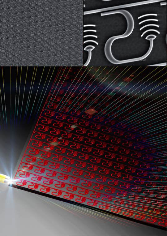
A large-scale nanophotonic phased array. Image by Jie Sun.
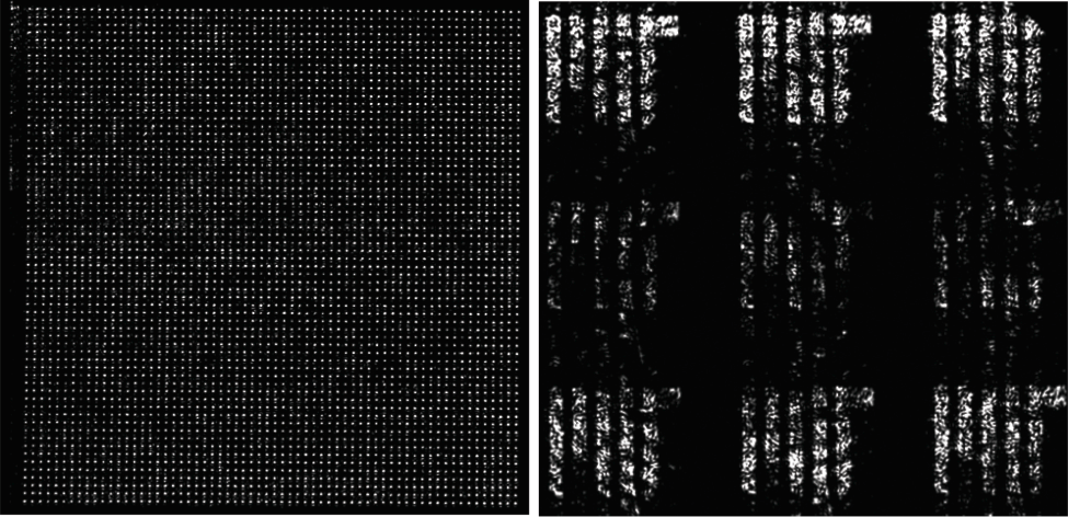
The emission plane (left) and image plane (right) patterns out of a 4096 element nanophotonic phased array designed to project the MIT-logo in the image plane. Image taken by Jie Sun.
Related Links: